Advanced Materials
for Electronics
We are Transene CO INC, founded in 1965 by Dr. Benjamin P. Hecht. Foremost in research and development of new materials for electronics and aerospace. Fields of interest encompass dielectrics, capacitors, photoresist materials, adhesives, photomask processing chemicals, conformal coatings, chemical etchants, electrolytic and electroless plating chemistries, encapsulants, and high purity cleaning compounds.
Our products find extensive use in semiconductor microelectronics, thin film and thick film hybrid microelectronic circuits, electronic components, photonics, LED, TFT, and other electronic applications.
TRANSENE COMPANY, INC. is competent and ready to help resolve technical problems and to engage in the development of special materials for our customers.
Please feel free to consult with us regarding your special materials problems.
Transene Company is committed to elimination of PFAS surfactants in our products. We partnered with UMASS Lowell and the TURI institute to identify and develop environmentally safer alternatives. We are proud of our collaborative effort and its positive effects. Additional information may be found here: https://www.uml.edu/news/stories/2022/transene-research.aspx
Nature Article: Could the world go PFAS-free?
CUSTOM SERVICES
 Transene offers complete custom and toll services in addition to our standard products. We are happy to work with your engineers and scientists to provide timely, cost-effective solutions to your company’s needs. Whether the quantity is one gallon or hundreds of gallons, Transene stands ready to manufacture according to your formulation or to customize one of our standard products to meet your unique application. Our technical staff will work with you to set up a procedure, devise quality control specifications, and prepare appropriate documentation and certification for the finished product. All custom products are treated with complete confidentiality. Click here to let us know how we can help with your custom or toll blending project or here to outline your custom R&D needs.
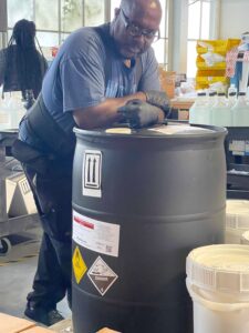
Transene’s Class 100 cleanroom packaging facility enables us to serve the exacting needs of the semiconductor industry. Combined with 0.2 micron filtration and ultrapure ingredients, our cleanroom allows us to ensure particulate-free products. Sizes from quart to drum are available. Transene is able to certify RoHS compliance and TSCA listing for our products.
COMMUNITY INVOLVEMENT
Transene Company is proud to partner with its employees in supporting the Martin E. Hecht Memorial Scholarship. Each year, funds raised are awarded to a graduating senior from Danvers High School who intends to pursue a college degree in a science or engineering discipline.
In addition, Transene has a history of supporting local schools through the donation of new and lightly used equipment and supplies. Providing support to our local communities is crucial to our role as good corporate citizens.
PARTNERS
Transene Company is proud to partner with KemLab, a leading-edge developer of photoresist materials designed specifically for use in photolithography.
![]()
Transene Company participates in the US Department of Homeland Security’s E-Verify program.
![]()
Customer Tools
Locations
Transene Company’s quality system is ISO 9001:2015 certified.
A copy of our quality policy is available upon request.
Click here for a copy of our ISO certificate