PKP-308PI Photoresist
DESCRIPTION
PKP-308PI Photoresist replaces PKP II and KTFR photoresists. This high purity photoresist offers improved resolution, adhesion, etch resistance, low pinhole density and best all-around properties available for negative-working resists. The need for membrane filtration of the photoresist in use is not essential. Resolution in the micron range is practical, while photoresist procedures will be found consistently reproducible in production. PKP-308PI resist is produced under conditions which assure high quality and comply with the critical and exacting requirements essential for advanced integrated circuit technology.
PKP-308PI product is purified by special processing based on a centrifuging technique under controlled isothermal conditions. The purification process yields photoresist material with excellent quality. The polymeric composition (cis-polyisoprene) shows uniformity in molecular weight and size distribution. In effect the centrifuging technique is a fractionation process with the very high molecular weight polymers removed. Consequently, resist films obtained from the purified products reveal very low pinhole density.
PKP-308PI PROPERTIES
| PARAMETER | SPECIFICATION | |
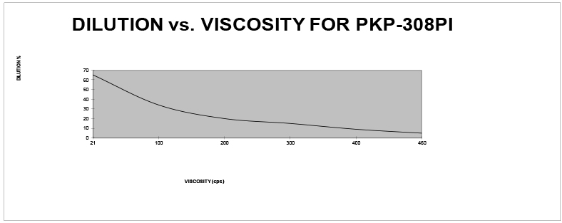
| Viscosity at 25 oC, mPa-S | 470-530 | |
| % Solids (by wt.) | 22-26 | |
| Water % | < 0.03 | |
| Application Test, 4,000 rpm | Thickness 4.8-5.4 mm | |
| Resolution 16-20 mm | ||
| Metals content, ppm | ||
| Calcium (Ca) | < 1 | |
| Chromium (Cr) | < 1 | |
| Copper (Cu) | < 1 | |
| Iron (Fe) | < 1 | |
| Lead (Pb) | < 1 | |
| Nickel (Ni) | < 1 | |
| Potassium (K) | < 1 | |
| Sodium (Na) | < 1 | |
| Zinc (Zn) | < 1 | |
| Shelf Life | 12 months | |
| Storage | Room temperature, avoid direct light | |
| Solvent | Xylenes | |
| Threshold Exposure Intensity (mj/cm2) | 15-25 | |
NOTE: For optimum adhesion of photoresist the equatorial spacing should correspond to lattice constant of substrate material: (Aluminum -4.0 Å: Silicon 5.4 Å ; SiO2 – 4.9 Å).
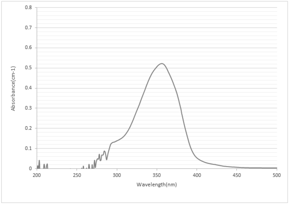
ABSORBANCE CURVE
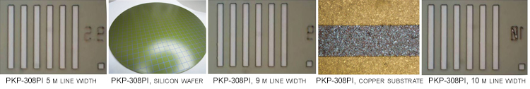
Dosage vs. Thickness on Copper Substrate

PKP-308PI – PRODUCT INFORMATION
INTRODUCTION: PKP-308PI eliminates many problems inherent in photoresist work. Through the Transene process of thermally controlled centrifugal filtration, a more uniform photoresist material relatively free of conglomerates has emerged. However, application and processing of photoresist films remain to some degree an empirical art. The following pages form a general outline of procedure for photoresist technology used throughout the industry. Yet, because environmental and equipment differences exist, it is usually, necessary to adjust conditions and process parameters until satisfactory results are obtained.
ENVIRONMENT: Several precautions are worthy of note:
- Dust and lint cause pinholes. These can be minimized by the use of clear-flow liquids.
- Relative humidity must be controlled between 30 – 50%.
- Appropriate lighting of gold fluorescent, yellow incandescent, or white fluorescent with yellow or orange filters must be used.
- Adequate ventilation is necessary because of solvent fumes.
STORAGE: PKP-308PI materials are purified expressly for your order. To remain conglomerate free, precautions must be taken:
- PKP-308PI materials should be stored away from light sources and not be removed from shipping bottles until used.
PROCESSING PROCEDURE:
- Substrate Preparation:
Clean and prebake 20-30 min. @ 120-130oC - Photoresist Application:
Motor-driven rotary spinning - Prebake (soft bake):
Hot plate: 90 seconds @ 90 oC
Oven: 30 minutes at 90 oC - Photoresist Exposure:
1-10 sec. minimum light source 15-25 mj/cm2 - Photoresist Develop:
10-60 second spray or 120 second immersion in PKP Developer followed by PKP Rinse (60-90 seconds immersion, 15 seconds spray) followed by compressed air or nitrogen blow-off. - Post-bake (hard bake):
Hot plate: 60 seconds @ 130 oC
Oven: 30 minutes at 130 oC - Photomask Stripper/Remover:
Transene Negative Resist Remover NRR-001 immersion at 50-60 oC for 3-5 minutes. Rinse with isopropyl alcohol if necessary
PHOTORESIST TECHNIQUE
- SUBSTRATE PREPARATION: Only if the substrate is perfectly clean and dry prior to resist application will a well-defined etch pattern free from defects be developed. Removal of surface particles and organic residues is accomplished by cleaning with solvent such as Transene 100 followed by baking at temperature between 120oC – 200oC for up to 20 minutes.
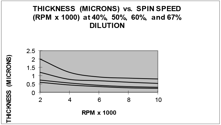
- APPLICATION: The standard technique of spinning a substrate on a motor driven rotary vacuum chuch yields the most uniform and reproducible thickness. Under this program centrifugal forces distribute a uniform coating of resist without significant solvent evaporation or excess resist being thrown off at the substrate edges. Begin by flooding substrate with photoresist. Never apply resist to substrate while spinning. An uneven distribution may result.Square or rectangular substrates are best coated at low rpm (50-1000 rpm). Undiluted resist at 75 rpm yields about 2.5 μ coatings, the substrate edges and corners being thicker.Circular substrates (the most common) are coated at high speed between 2,000 – 5,000 rpm, resulting resist thickness being determined by resist viscosity, rpm and acceleration. RPM speed > 5,000 has little effect on resist thickness. The lower the viscosity of a resist, the less revolution speed (rpm) affects coating thickness. Time of acceleration to peak rpm is generally regarded to be the determinant of thinner and more uniform thickness across the substrate. Also, the slightly thicker resist coating at the edge of the substrate is reduced. The optimum acceleration time to attain peak rpm is 0.1 sec.Resist film thickness used for thin film circuits vary from 0.3 to 2 μ. At lower thickness limits, dilution of resist can cause a discontinuous film. Thick films (1-2 μ) give added protection against etch penetration and pinhole formation at the expense of less resolution. A better approach of spinning two thin coats results in assured quality and desired thickness of resist films.
- PREBAKING: Evaporation of residual solvents results in maximum adhesion of resist to substrate. Resist coatings not thoroughly baked will have variable exposure requirements because residual solvents will inhibit cross linking of functional groups. Excessive baking may also create problems such as fogging and decomposition of resist material. Bake-out time is dependent upon film thickness.
- EXPOSURE OF PHOTORESISTS: Photoresists may be exposed with any light source having output in the near UV spectrum. Large-area light sources are used only for coarse (50 μ or 0.002 inch or larger) lines. To resolve fine details a less diffused light source is necessary. Generally, for fine lines patterns point sources (carbon arc, high pressure mercury vapor or Xenon flash lamps) are used at a point remote from substrate.This will insure uniformity of light intensity across substrate. Proper exposure of PKP-308PI requires light energies of about 15-25 mj/cm2. Correct exposure is dependent upon thickness and processing variables. An exposure of 1-10 seconds is sufficient providing the light source is capable of yielding minimum irradiation intensity of 10mj/cm2 at substrate surface.For good fine-line definition and reproducibility, the exposure energy must be controlled within 10% of the optimum value. Light intensity at the substrate surface should be monitored. Due to diffraction effects of resist material, overexposure produces cross linking of resist under the mask, the effect being line broadening to as much as 2.5 μ.Underexposure resulting in cross-linking only at the surface of the resist film can cause the pattern to be washed off when the image is developed. Line broadening can also be the fault of substrate irregularity and/ or insufficient contact between mask and resist surface. The use of a vacuum to hold the mask against a perfectly smooth substrate will solve this problem.The PKP-308PI sensitizer decomposes without cross-linking the polymer if exposure takes place in the presence of oxygen. This reaction is limited only to the surface of the film, which remains soluble in the developer. This oxygen effect will not be noted in working with resist coatings of > 1 μ. Film coatings of 0.5 μ or less may be affected greatly, not offering enough protection in the subsequent etch operation.
- PHOTORESIST DEVELOPMENT: In general, the best procedure involves a 10 to 60 second spraying of the developer onto the coated substrate. Follow this with several non-aqueous rinses (isopropyl alcohol). Using pure compressed air or nitrogen residual solvent is blown off the surface. Transene PKP Developer is recommended.
- POSTBAKING: Post baking of the developed resist will evaporate residual solvents, enhance chemical stability of the polymer coat, and further enhance adhesion.
- PHOTORESIST REMOVAL: A hot (60o) solution of Transene Negative Resist Remover NRR-001 is an efficient stripper for PKP-308PI resist.
Customer Tools

Locations
Transene Company’s quality system is ISO 9001:2015 certified.
A copy of our quality policy is available upon request.
Click here for a copy of our ISO certificate