Cleaning Surfaces – Polishing
Waxcut
Waxstrip L2X
Transene –100
TUD – Transene Ultrasonic Detergent
Lab Glass Cleaner
Transene Glass Cleaner- 409
Transene Flux Remover/Degreaser TFR220-DG
ESP
Polimet
Polmet
Sequestrox
Semiconductor Grade Deionized H2O (Ultra Pure)
Gold/Silver Cleaner
WAXCUT
DESCRIPTION
Waxcut is an environmentally safe powder compound prepared primarily for the removal of mounting waxes in semiconductor processing. In addition to its ability to solvate waxes and oils, Waxcut can be used for removal of silicones, greases, soils, finishing compounds, and normal contaminants. Waxcut is compatible for use on iron, silicon, glass, aluminum zinc, brass, copper, and magnesium. Waxcut is ideal for cutting beeswax, stacking wax, and high-rosin content waxes such as Hughes wax.
APPLICATION
- Add 6 oz Waxcut (approximately 170 grams) to one gallon of water and allow to dissolve completely.
- Bring solution to a temperature of 50 o C to 70 o C and immerse parts to be cleaned.
- Rinse parts thoroughly.
NOTE: Ultrasonic agitation greatly enhances the cleaning process and reduces cleaning time.
WAXSTRIP L2X
DESCRIPTION
Waxstrip L2X is an environmentally safe concentrate prepared primarily for the removal of mounting waxes in semiconductor processing. In addition to its ability to solvate waxes and oils, Waxstrip L2X can be used for removal of silicones, greases, soils, finishing compounds, and normal contaminants. Waxstrip L2X is compatible for use on iron, silicon, glass, aluminum zinc, brass, copper, and magnesium
APPLICATION
- Combine Waxstrip L2X with deionized water in equal amounts.
- Bring solution to a temperature of 50 o C to 70 o C and immerse parts to be cleaned.
- Rinse parts thoroughly.
NOTE: Ultrasonic agitation greatly enhances the cleaning process and reduces cleaning time.
Available in 1 gallon, 5 gallon, or 55 gallon units
Transene 100®
For Ultra Clean Surfaces
Removes foreign substances and contaminants from semiconductor surfaces.
Patent Citation Referencing Application of Transene 100
FEATURES
- Stabilization of semiconductor devices through clean surfaces
- Overcomes soft reverse characteristics when due to surface contaminants
- Generates higher yield of p-n junction devices
- Useful for final cleaning process before thermal oxidation of silicon, diffusion and after p-n junction etches
TRANSENE 100
What is TRANSENE – 100
TRANSENE-100 is a novel chemical product designed for use in the semiconductor industry to improve quality, yields, and reliability of p-n junction devices. It is especially applicable to transistors, diodes, rectifiers, and integrated circuits. TRANSENE-100 serves to establish clean surfaces and ensure surface stabilization of semiconductor devices when it is properly used.
PROPERTIES OF TRANSENE 100
| Boiling point range | 75 ° to 101 °C |
| Specific Gravity | .75 |
| Heavy Metals | < 0.35 ppm |
| Particulate matter | None (visually) |
| Acidity | Neutral |
| Flash Point | 70 ° to 75 °F |
| Contact Hazard | Very slight irritant, not dangerous |
| MAC | 400 parts per million |
| Fire Hazard | When exposed to flame |
| Ventilation control | Normal ventilation rate, use of hood preferred |
| Spontaneous combustion | No |
| Toxic hazard | Narcotic systemically |
How TRANSENE-100 Works
The primary function of Transene-100 is to remove foreign substances found on semiconductor surfaces. These substances may be loosely held on the surface, or they may be absorbed electrolytes or precipitated metals. Water, alcohol, acetone, and other solvents fail to remove them efficiently or else not at all. TRANSENE-100 is efficient in breaking van der Waals forces responsible for tenacious binding of some foreign substances. TRANSENE-100 is also capable of removing substances absorbed on semiconductor surfaces. In general, much surface contamination can be extracted by use of TRANSENE-100. This product, however, is not a chemical etch, and not intended as a substitute for chemical etching.
Why use TRANSENE-100
Surface cleanliness has a very special meaning in the manufacture of semiconductor products. The presence of foreign material at junction sites may lead to highly localized fields where current is drawn through by Zener tunneling, resulting in high reverse currents. The occurrence, even in minute trace quantities, of ions, electrolytes, or metal impurities on semiconductor surfaces causes poor device electrical characteristics such as hysteresis, flutter, and high leakage current. Mobile ions located anywhere on the active device surface will affect ultimate device reliability, particularly at high temperature operation. With TRANSENE-100 a relatively clean surface characterized by stable surface states is produced.
How TRANSENE-100 is used
AFTER ETCHING – Treatment with TRANSENE-100 is performed after chemical or electrolytic etching is carried out, but prior to the bake out, varnish coating, or final encapsulation and sealing of p-n junction devices.
The semiconductor devices, following the etching and rinsing operations, should be placed in a beaker with sufficient TRANSENE-100 covering them and then heated on a hot plate. Five minutes of gentle boiling generally suffice. The semiconductor devices are then removed. TRANSENE-100 is completely volatile and leaves no residue. In this respect, it is much purer than water or other solvents commonly used. The TRANSENE treated devices are now ready for final bakeout, coating, and sealing as may be customarily performed.
PRE-OXIDATION and DIFFUSION – TRANSENE-100 is especially recommended for the final cleaning treatment before thermal oxidation of silicon and diffusion processes to remove surface contaminants. These contaminants if not removed may lead to pinholes in the oxide passivation layer and faulty diffusions.
TUD®
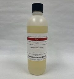 Transene Ultrasonic Detergent
A powerful detergent solution for ultrasonic cleaning electronic parts and semiconductor materials.
SPECIAL FEATURES
- All purpose cleaner
- High sequestering power
- Enhanced ultrasonic detergent action
- Good rinsability
- Economical: used as a liquid concentrate
TUD® – Transene Ultrasonic Detergent
DESCRIPTION
Transene Ultrasonic Detergent (TUD) is a general purpose cleaner used for silicon and other semiconductor materials soiled in slicing, lapping or polishing. It is also used to clean electronic parts. The detergent formulation is multiple acting with especially good solvent action. It exhibits high sequestering ability, very strong surface activity, suspension and emulsification properties. Surface contaminants normally resistant to conventional detergents are readily removed.
The detergent power is based on a balanced product formulation. Highly active surfactants reduce surface tension below 35 dynes/cm. An effective hydrophilic-hydrophobic balance is maintained. As a result of the detergent-water interface, which penetrates around soils and surface contaminants, ultrasonic action in cleaning is enhanced.
Phosphates and polyphosphates present as inorganic builders in optimized concentration add to the detergency and provide proper pH and buffer capacity.
Glycol ether solvents blend with water to extend solvent action to a variety of soils and contaminants. This lends the formulation its unique ability to remove wax, scums, greases and other hydrophobic soils.
Chelating agents are purposely added to complex heavy metal impurities. The product is not sensitive to hard water because of the water-softening agent.
Coupling materials or hydrotropes are also added to insure stability over a range of temperature conditions. Finally, a non-ionic water-soluble thickening agent is used to impart the desired viscosity.
TUD contains approximately 5% VOC.
APPLICATION
Transene Ultrasonic Detergent (TUD) is supplied as a liquid concentration to be diluted with water – 4 ounces of the concentrate is used to make one gallon of detergent solution. The solution is used hot or at room temperature, preferably ultrasonically, for rapid, efficient cleaning. Excessive sudsing will not be encountered. The detergent is readily rinsed off with demineralized water.
Lab Glass Cleaner LGC-300
DESCRIPTION:
Transene LAB GLASS CLEANER LGC-300 is specifically formulated for maintenance of semiconductor clean room equipment and glassware. Safe to use on glass, aluminum, copper, stainless steel, silicon, teflon, rubber, and most plastics.
FEATURES:
- VLSI standards 0.2 micron filtration
- Low sodium: < 2.0 ppm
- Non-streaking
- 100% water soluble concentrate
- Soak or spray cleaner
PROPERTIES:
| pH | 9 |
| Boiling Point | 93 °C |
| Freezing Point | 0 °C |
| Residue | None |
| Toxicity | Non-toxic/non-flammable |
APPLICATION:
TRANSENE LAB GLASS CLEANER LGC-300 is supplied in concentrate form. One pint concentrate added to seven pints distilled water makes one gallon of cleaning solution. Most surfaces may be cleaned simply by application: spray or soak. For more difficult cleaning tasks or small, hard-to-reach areas of labware, an elevated temperature soak followed by a water rinse is recommended.
TRANSENE GLASS CLEANER 409
DESCRIPTION:
TRANSENE GLASS CLEANER 409 is specifically formulated for maintenance of semiconductor clean room equipment and glassware. Safe to use on glass, aluminum, copper, stainless steel, silicon, teflon, rubber, and most plastics. Transene Glass Cleaner 409 is an excellent general purpose cleaner for any laboratory environment. Glass Cleaner 409 contains a chelating agent to remove metal ionics.
FEATURES:
- Low VOC
- Low sodium: < 2.0 ppm
- Non-streaking
- 100% water soluble concentrate
- Soak or spray cleaner
PROPERTIES:
| pH | 9 |
| Boiling Point | 98 °C |
| Freezing Point | -5 °C |
| Residue | None |
| Toxicity | Non-toxic/non-flammable |
APPLICATION:
TRANSENE GLASS CLEANER 409 is supplied ready to use. Most surfaces may be cleaned simply by application: spray or soak. For more difficult cleaning tasks or small, hard-to-reach areas of labware, an elevated temperature soak followed by a water rinse is recommended.
TRANSENE FLUX REMOVER TFR-220DG
DESCRIPTION:
TRANSENE FLUX REMOVER/DEGREASER TFR-220DG is a versatile, ozone-safe flux remover and degreaser designed for cleaning printed circuit boards, connectors, and hybrids. TFR-220DG is a proprietary blend of aliphatic hydrocarbons which effectively removes all flux types including synthetic, water soluble, rosin, and no-clean fluxes in addition to grease.
The mild odor of TFR-220DG lends itself to large scale processing of PCBs, stencils, gaskets, housings, wiring harnesses, and other electronic components. With both hydrophobic and hydrophilic activity, TFR-220DG removes both organic and ionic deposits. No rinse is required as TFR-220DG dries residue-free. Transene TFR-220 is non-flammable and degrades to environmentally safe materials.
FEATURES:
- Zero Ozone Impact
- High Purity
- Residue Free
- Removes All Flux Types
- Degreaser
PROPERTIES:
| Viscosity | < 100 cps |
| Boiling Point | 150 °C |
| Flashpoint | 44 °C (TCC) |
| Residue | None |
| Surface Tension | 17 dynes/cm |
| Specific Gravity | 0.82 g/cc at 25 °C |
| Water Solubility | 60% by weight |
| Evaporation Rate | 0.15 (butyl acetate = 1) |
| Toxicity | Non-toxic |
ESP®
Electroless Silicon Polish
Chemical-Mechanical Polishing Process for Silicon
FEATURES
- Polishes silicon without use of abrasive
- High speed polishing rates obtainable
- Polished surfaces free of work damage, orange-peel effects, or pitting
- Surfaces are left clean, nearly crystallographically perfect
- Also polishes germanium and other semiconductor materials
ESP® ELECTROLESS SILICON POLISH
DESCRIPTION
ESP is an electroless, silicon-polishing process based on copper-polyfluoride chemistry. It offers a simple yet productive method for the preparation of highly polished silicon. The process is especially useful to obtain silicon substrates for diffusion work and for epitaxial deposition.
The polishing process is accomplished by placing silicon wafers in contact with a polishing wheel covered with a suitable polishing cloth. ESP solution is permitted to saturate the polishing cloth, while silicon atoms undergo chemical displacement by copper ions. The copper deposit is sequentially removed from the silicon surface by wiping action of the polishing wheel. Under optimized polishing conditions, removal of copper takes place as readily as copper deposition occurs. The polishing process is greatly enhanced by the special buffered composition of ESP, containing polyfluoride ions. The overall ionic reaction for the polishing process is
Cu +2 + Sio + 6F–+ 2(NH4)+ > 2Cuo + ( NH4) 2SiF6.
Polished silicon obtained by the ESP process is of excellent quality, very much superior to conventional chemical or mechanical polishing methods. ESP leaves the surface clean, flat and nearly crystallographically perfect. Furthermore, the polished surfaces are free of work damage, pitting or orange-peel effect. Resistivity rings are also absent as the process is not greatly affected by acceptor or donor impurities present in the silicon material.
PROPERTIES OF ESP
| Appearance | Clear, blue solution |
| pH | 5.25 ± .05 |
| Critical Polishing Pressure | 2 psi |
| Working Pressure | 2.5 – 3 psi |
| Polishing Wheel Speed | 75 rpm |
| Polishing Wheel | Pellon pan W cloth or leather |
| Operating Temperature | 25 °C |
| Polishing Rates | |
| @ 25 °C | 2 mils/hr. |
| @ 40 °C. | 4 mils/hr. |
| Shelf Life | 4 months |
Polimet – Alumina Type
Polishing Lapping Preparations
Metallurgical lapping and polishing with aluminum oxide in a liquid polyol carrier base, special antistatic agent included.
UNIQUE ADVANTAGES
- Facilitates lapping and polishing procedure
- Provides non-drying liquid vehicle
- Accelerates abrasive action
- Eliminates static charge phenomenon
- Affords effective particle size distribution of lapping and polishing compounds for specific requirements and needs
- Scratch-free, polished surfaces
POLIMET Alumina Type
DESCRIPTION
POLIMET lapping and polishing preparations are suspensions of optical finishing grades of pure aluminum oxide powder in a polyol-water base, antistatic agent included. The particle size distribution for the dispersed medium is held extremely close. The polyol-water base, furthermore, is essentially non-drying and the presence of an antistatic agent prevents static charge accumulation during metallurgical polishing. In addition, the preferred and selected crystal structure of aluminum oxide assures rapid cutting, while the polyol-water base provides smooth polish, less damage, and scratch-free surfaces. Also available in paste form.
POLIMET, alumina type, is recommended for metallurgical polishing of metals, semiconductors, glass polymeric materials; etc. The use of POLIMET – A, B, and C produces a very high polish of exceptional quality. POLIMET – D, E, F, G and H are suitable for abrasive cutting and lapping.
POLIMET PREPARATIONS, ALUMINA TYPE
| Alumina Type | Micron Size | Crystal Structure | Hardness, Mohs | Purpose |
| POLIMET –A | 0.05 | Cubic | 8 | Polishing |
| POLIMET –B | 0.3 | Hexagonal | 9 | “ |
| POLIMET –C | 1.0 | “ | 9 | “ |
| POLIMET –D | 5.0 | “ | 9 | Lapping |
| POLIMET –E | 10.0 | “ | 9 | “ |
| POLIMET –F | 15.0 | “ | 9 | “ |
| POLIMET –G | 20.0 | “ | 9 | “ |
| POLIMET –H | 25.0 | “ | 9 | “ |
INSTRUCTIONS
Conventional procedures for metallurgical polishing should be followed, through specific instructions can be provided for polishing various materials.
Polmet Alumina Type
Polishing and Lapping Compounds
Electronic grades of alumina abrasive compounds specially processed to meet requirements for critical surface preparation in lapping and polishing processes.
FEATURES
- High purity alumina with hexagonal crystal structure
- Effective particle size distribution
- Rapid abrasive action
- Ultra high polish
- Meets ASTM requirements
IMPORTANT APPLICATIONS
For lapping and polishing – germanium, silicon, intermetallics, ceramics, ferrites, laser crystals, optical glass lenses, plastic contact lenses, windows, stainless steels, and metallographic specimens.
POLMET Alumina Type
DESCRIPTION
Polmet lapping and polishing products are white, pure, alumina compounds, occuring in the hexagonal crystalline state. These compounds possess a high degree of hardness (9 Mohs) and are further characterized by very uniform particle size distribution. Polmet polishing and lapping compounds are unmatched for critical lapping and polishing operations.
Grades of Polmet compounds are based upon particle size and are offered to meet exacting requirements in surface preparation.
| GRADES | MICRON SIZE | APPLICATION |
| Polmet-alpha | .05 | High-polish |
| Polmet-beta | .3 | High-polish |
| Polmet-gamma | 1 | Polish |
| Polmet-delta | 3 | Very fine lapping |
| Polmet-epsilon | 5 (2,500) | Fine lapping |
| Polmet-zeta | 10 (1,250) | Lapping |
| Polmet-eta | 12 | Lapping |
| Polmet-iota | 15 | Coarse lapping |
| Polmet-kappa | 20(600) | Coarse lapping |
| Polmet-lambda | 25 (500) | Coarse lapping |
| Polmet-mu | 30 (400) | Coarse lapping |
Corresponding mesh size in parenthesis.
Also available in slurry form. See Bulletin No: 116 – Polimet Alumina Preperations
APPLICATION
Polmet aluminas are used in water slurries, paste forms and in oil suspension for lapping and polishing processes. Standard cloths, plastics, and proprietary lapping and polishing plates are in common use.
Sequestrox
Residue Removers for Low K Dielectric and Silicon Devices
Effective oxidizing and chelating systems used to remove ash residue from low k dielectric materials and to stabilize etched silicon p-n junction devices by removing etch contaminants.
SPECIAL FEATURES
- Lead to chemically clean surfaces
- No etching of substrate
- Low leakage junction characteristics
- Sharp avalanche breakdown
- Stable, high temperature electrical characteristics
- High product yield
- Non-hazardous
- Water-rinse
Sequestrox Ash Residue Removers for Low K Dielectrics
DESCRIPTION
Sequestrox has been reformulated to support the drive toward sub – 0.25 m technologies. Manufacturers require residue removers to clean vias, metal lines, and trenches of ash or metal etch residues. Residue results from the etch process and can interfere with device yield and performance.
Sequestrox systems employ proprietary chemistry to complex and chelate residue and contaminants. Sequestrox Types I – IV are sodium free, and all systems are readily rinsed with deionized water. No intermediate rinse is required. Sequestrox chemistry is mild and exhibits low etch rates on sensitive metals.
BENEFITS
- Low temperature processing
- Compatible with most low-k films
- Aqueous, non-hazardous
- Low oxide etch rates
- Sequestrox Types I, II, and III are compatible with Ag, Cu, and Ni.
- Sequestrox Type IV is compatible with Mo, W, Ag, Al, Cu, and steel.
APPLICATION
Sequestrox systems are compatible with HDPE, LDPE, PP, rubber, and teflon coated materials.
Sequestrox Type I, II, and III
-
- Step 1. Pre-mix equal volume of Sequestrox – Type I and II solutions. Expose assemblies immediately to the mixture and clean ultrasonically for 1 to 2 minutes.
- Step 2. Add Sequestrox – Type III solution (10 ml to 100 ml mixture of Sequestrox – Type I and Type II as used above) and ultrasonically clean for additional one-half minute. Rinse in deionized water.
Sequestrox Type I & II for copper and nickel
-
- Step 1. Pre-mix equal volumes of Sequestrox – Type I and II solutions. Immediately expose the assemblies to the mixture and clean ultrasonically for 1 to 2 minutes.
- Step 2. Rinse in deionized water. Then complete cleaning in acetone ultrasonically or preferably in Transene 100.
Sequestrox Type IV for tungsten and molybdenum
-
- Step 1. Silicon assemblies are exposed to Sequestrox solution Type IV ultrasonically at room temperature for 3 minutes.
- Step 2. Rinse in deionized water, then in acetone ultrasonically or Transene 100.
Sequestrox Etching Adjuncts for Silicon Devices
DESCRIPTION
Sequestrox systems are specially formulated electrolyte compositions which are used in conjuction with etch processes in the manufacture of silicon p-n junction devices to improve quality and yield. The standard etch process (nitric-HF-acetic) performs the requisite removal of damaged silicon, though invariably the etching leaves residual surface contaminants. These impurities originate from etch solutions and from various exposed metal parts of the silicon device. The complete removal of these contaminants must be practiced to avoid device failure. This can be accomplished with Sequestrox systems as etching adjuncts.
Sequestrox systems involve the use of agents which effectively oxidize, complex and chelate the surface contaminants occurring on silicon. Sequestrox systems are sodium free and readily removed by rinsing in deionized water. Several systems are offered with selectivity based upon the type of metal parts comprising the silicon device assembly.
SEQUESTROX – Type I, II, and III
Recommended in the etch process for semiconductor assemblies with silver and copper parts, lead-tin or other solders and nickel plated silicon.
SEQUESTROX – Type IV
Recommended in the etch process for semiconductor assemblies with molybdenum and tungsten contacts, silver, aluminum, copper and steel parts.
APPLICATION
In general, the application of Sequestrox systems follows the conventional acid etch performed to remove the mechanically damaged silicon of p-n junction devices. The appropriate Sequestrox system must be selected and used. Typical procedures for using Sequestrox as an etching adjunct follow:
SEQUESTROX – Type I, II, and III
(Silicon rectifier assemblies with silver leads)
-
- Step 1. Etch assemblies in nitric-HF-acetic acid mixture to remove edge damage. Rinse in deionized water.
-
- Step 2. Pre-mix equal volume of Sequestrox – Type I and II solutions. Expose assemblies immediately to the mixture and clean ultrasonically for 1 to 2 minutes.
-
- Step 3. Add Sequestrox – Type III solution (10 ml to 100 ml mixture of Sequestrox – Type I and Type II as used above) and ultrasonically clean for additional one-half minute. Rinse in deionized water.
- Step 4. Complete cleaning process with acetone ultrasonically or preferably with Transene-100.
SEQUESTROX – Type I and II
(Silicon rectifiers, copper stud mounted)
-
- Step 1. Silicon dice pre-etched in nitric-HF-acetic before mounting.
-
- Step 2. Pre-mix equal volumes of Sequestrox – Type I and II solutions. Immediately expose the assemblies to the mixture and clean ultrasonically for 1 to 2 minutes.
- Step 3. Rinse in deionized water. Then complete cleaning in acetone ultrasonically or preferably in Transene 100.
SEQUESTROX – Type IV
(Silicon rectifiers with molybdenum contacts)
-
- Step 1. Silicon is pre-etched and mounted, or silicon with the contacts is spin-etched to remove damaged silicon of p-n junctions.
-
- Step 2. Silicon assemblies are exposed to Sequestrox solution Type IV ultrasonically at room temperature for 3 minutes.
- Step 3. Rinse in deionized water, then in acetone ultrasonically or Transene 100.
| SEMICONDUCTOR GRADE DEIONIZED H2O (Ultra Pure) |  |
DESCRIPTION
Transene’s Ultra Pure – Semiconductor grade deionized water has been pretreated by a combination of reverse osmosis (RO) and electrodeionization. The water is further purified through carbon cartridges removing dissolved organic contaminants and residual chlorine and a deionizer cartridge removing dissolved inorganic contaminants. A final filter unit removes any microorganisms larger than 0.22 microns. Transene’s water meets ASTM Type I specifications.
PROPERTIES:
| Resistivity: | 18.2 MΩ.cm |
| 0.05 Micron Filtered | —– |
APPLICATION
The high quality water produced is suitable for critical applications in the electronics industry.
Resistivity: 18 Meg-ohm-cm, 0.05 micron filtration
Transene’s Ultra Pure – Semiconductor grade deionized water has been pretreated by a combination of reverse osmosis (RO) and electrodeionization. The water is further purified through carbon cartridges removing dissolved organic contaminants and residual chlorine and a deionizer cartridge removing dissolved inorganic contaminants. A final filter unit removes any microorganisms larger than 0.22 microns.
The high quality water produced is suitable for critical applications in the electronics industry.
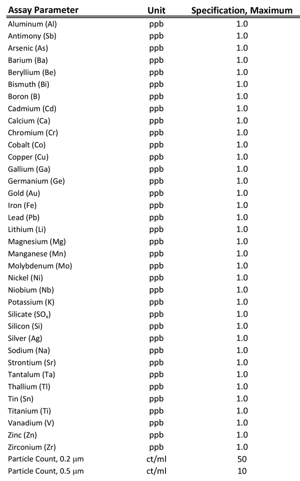
TYPICAL TRACE METALS ANALYSIS (ppb)
GOLD/SILVER CLEANER
DESCRIPTION:
Removes oxides and tarnish from gold, silver, and precious metal alloy surfaces without leaving a residue. Gold/Silver Cleaner is recommended for cleaning metal films immediately prior to further processing. Gold/Silver Cleaner is an effective surface activator and adhesion promoter for gold and silver substrates prior to bonding processes.
FEATURES:
- Rapid, economical cleaning
- Enhances fluxing, soldering, etching, plating, and coating
- No adverse electrical effects
- Mild pH
- Compatible with most metals
- Non-aggressive formulation
- Cyanide-free
PROPERTIES:
| Tank | Pyrex glass, fiberglass, polypropylene, etc |
| Temperature | 20-50 °C |
| Immersion Time | 30-60 seconds or as needed |
| Rinse Use with agitation |
Water |
APPLICATION:
Substrates should be degreased first, if necessary
Customer Tools
Locations
Transene Company’s quality system is ISO 9001:2015 certified.
A copy of our quality policy is available upon request.
Click here for a copy of our ISO certificate